 |
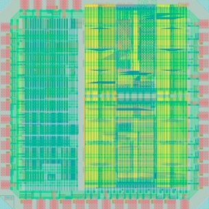
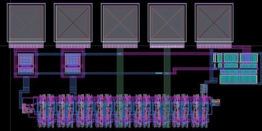
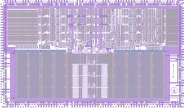
TrueNorth: a single chip million spiking neuron system (design 2011-2013; chips 2013)
Process: 28nm
A low power million spiking neurons/chip neuromorphic system with scalable communication (joint project with IBM research).
Highlight: First single chip million neuron neuromorphic architecture. Fully digital, deterministic, highly programmable neurons, synapses, and communication with a glueless chip-to-chip network and less than 70mW power. Hybrid QDI and bundled data asynchronous design, with a low frequency clock for 1:1 correspondence to a parallel discrete event software model. 4096 cores and 5.4 billion transistors makes this the largest asynchronous chip, and one of the largest chips ever designed.
|
 |
GPS baseband (design 2010-2013; chips 8/2013)
Process: 90nm
A low power GPS baseband processor
Highlight: An asymmetric self-timed baseband processor that uses 1.4mW for continuous tracking of 6 channels with 3D RMS error less than four
meters.
|
 |
Ultra low power embedded processor (design 5/2012; chips 9/2012)
Process: 90nm
Design of a low power microcontroller for embedded systems.
Highlight: Capable of operating at >90MIPS for <5mW in 90nm.
|
 |
Split-foundry AFPGA (design 10/2012; chips 2/2013)
Process: 0.13μm split foundry
Design of a chip using split-foundry technology, where the FEOL plus initial metallization
is completed at one foundry, with the BEOL completed at a second foundry.
Highlight: The first FPGA (and one of the first complex digital ASICs) in a split-foundry process. The layout of the chip was automatically generated even though the circuits are custom. This was done through dynamic cell generation, rather than technology mapping to standard cells.
|
 |
Digital neurosynaptic core (design and chips 2010)
Process: 45nm SOI
A programmable event-driven digital core for neuromorphic systems
(joint project with IBM research).
Highlight: a new approach to neuromorphic system design using a cross-bar based synapse organization
for increasing synaptic density as well as managing communication fanout.
|
 |
3D characterization (design 10/2006; chips 9/2007)
Process: 0.18μm SOI + 3D
Characterization of thermals and process variation in Lincoln Labs' 3D process.
|
 |
3D AFPGA (design 4/2005; chips 6/2006)
Process: 0.18μm SOI + 3D
3D asynchronous FPGA with three tiers in Lincoln Labs' 3D process.
|
 |
SNAP microprocessor (design 2001-2005; chips 6/2005)
Process: 0.18μm
A dual-use asynchronous microprocessor:
(i) An ultra low power processor for sensor network applications;
(ii) A high-performance wireless network simulator.
Highlight: The first microprocessor for sensor networks.
|
 |
Asynchronous FPGA (design 2003-2004; chips 6/2004)
Process: 0.18μm
A pipeline-level programmable dataflow asynchronous FPGA (AFPGA).
Highlight: The fastest CMOS FPGA. The first complete tool-chain for
asynchronous FPGAs.
|
 |
Low temperature characterization (design/chips 2007)
Process: 0.5μm SiGe
Demonstration of asynchronous circuit operation from 40K-400K for NASA's
Extreme Environment Electronics program.
|
 |
MiniMIPS (design: 1995-1998; chips 1/1999)
Process: 0.6μm
Andrew Lines, Rajit Manohar, Mika Nystrom, Robert Southworth, Paul Penzes, Uri Cummings, Tak-Kwan Lee, Alain Martin
A high-performance asynchronous MIPS processor.
Highlight: The fastest asynchronous microprocessor. One of the fastest
integer cores (academic or commercial) in 0.6μm
|